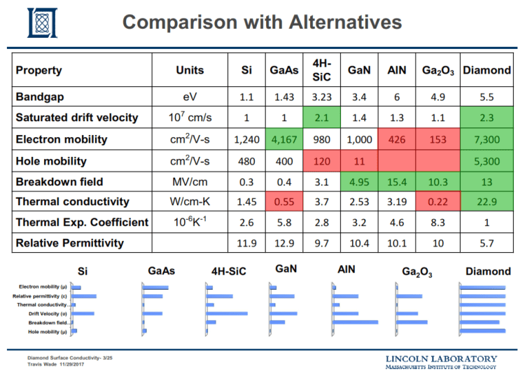
Diamond’s potential as an electronic material has become legendary by virtue of its wide band gap (5.5eV), high carrier mobility, breakdown field, saturation velocity, and thermal conductivity. If this potential can be realized, diamond is ideally suited as the material for devices which operate at high temperatures, voltages, power levels, and frequencies, as well as in high-radiation environments. The electrical resistivity of natural diamond is as high as 1015 ohm-cm and that of homoepitaxial CVD diamond films is equally high. The potential of diamond as a material for solid state devices has been the subject of a number of reviews [1-4].
As a semiconductor, the properties of diamond (except for electron mobility) are virtually unexcelled. Of semiconductors currently in use, only germanium (Ge) and indium antimonide (InSb) exhibit superior hole mobilities. Even then, these materials exhibit poor saturated hole velocities and low dielectric strength.
The wide band gap (5.5ev) of diamond simultaneously makes it an excellent insulator and an unusably resistive semiconductor. With doping, the intrinsic properties of diamond can be manipulated into practical energetic states. Boron has been identified as the dopant responsible for p-type behavior in naturally occurring semiconducting diamond [2]. From geometric and energetic considerations, boron is likely the only element that can substitutionally dope diamond without large distortions to the lattice. Nitrogen, a commonly occurring impurity in diamond, is electrically inactive, although it acts as a recombination center [2]. A theoretical study by Kajihara et al [8] suggests the potential of P, Li, and Na as shallow n-type dopants. Phosphorus is theorized to occupy a substitutional site, while lithium and sodium are expected to reside in interstitial positions. Recent work on phosphorous doping has met with some success [9].
CVD deposited diamond films necessarily contain hydrogen, as it is an essential component of the plasma growth environment. Hydrogen is known to reduce the resistivity to the order of 106 Ω-cm. Annealing in a hydrogen-free environment allows hydrogen to diffuse out of the film, increasing resistivity by a few orders of magnitude [10, 11]. Exposure to hydrogen reversibly reduces the resistivity to as-deposited values. An improved understanding of hydrogen effects in diamond films would certainly contribute to tighter control over electrical properties.
Surface conductivity of diamond has been established as a method by which to achieve useful electron density and mobility and still leverage the superlative properties of diamond.
Diamond’s properties (highest thermal conductivity, high hole & electron mobilities, & high electric breakdown field) predict that diamond field‐effect transistors (FETs) will have superior high‐power high‐frequency performance over FETs formed in other semiconductors.

The development of diamond FETs is limited by a lack of quality substrates and the high ionization energy of the primary dopant, boron (B). This high ionization energy results in very low levels of carrier activation at room temperature. Since only active carriers move charge, but all dopants increase scattering, this commonly contributes to a resistibity too high for FETs.
Fortunately, recent developments are addressing these shortcomings. Single‐crystal diamond substrates ≈4 inches have been demonstrated via heteroepitaxy. Diamond growth by heteroepitaxy, thus far, has a significant defect density disadvantage to diamond grown on existing diamond (homoepitaxy). Because many of these individual defects are based on the dislocation of one or a few atoms, some applications will be insensitive to their presence. However, electronics applications dependent on diamond’s wide bandgap are particularly sensitive to many of these types of defects and the associated electronic states they create.
At least two approaches are currently being pursued to address the dopant issue. When the surface of diamond is terminated in H, a surface p‐type conductive layer can form. FETs designed to exploit this layer demonstrate competitive high‐frequency performance, though manufacturability of this type of device has yet to be worked out. The second solution to doping uses delta doping by B. The concept of delta doping suggests that a heavily doped layer with an extremely sharp doping layer boundary can induce conduction in an adjacent undoped region. The net result can be a high carrier density consistent with the doped layer and simultaneously attain the high mobility possible in the undoped layer. In diamond, researchers have achieved a thin <2‐nm layer doped with boron at >1020 cm−3 is sandwiched within undoped diamond. This structure mitigates boron’s high ionization energy by producing an acceptor sub-band with ≈100% boron ionization. Recent reports of delta‐doped diamond have channel resistances suitable for device applications.
1. Keyes, R.W., Figure-of-merit for semiconductors for high speed switches. Proc. IEEE, 1972. 60.
2. Collins, A.T. and Lightowlers, E.C., The Properties of Diamond, ed. J.E. Field. 1979, San Diego: Academic Press.
3. Shenai, K., Scott, R.S., and Baliga, B.J., Optimum Semiconductors for High Power Electronics. IEEE Transactions on Electron Devices, 1989. 36.
4. Geis, M.W., Efremow, N.N., Woodhouse, J.D., et al., Diamond cold cathode. Electron Device Letters, IEEE, 1991. 12(8): p. 456-459.
5. Trew, R.J., Yan, J.B., and Mock, P.M., The potential of diamond and SiC electronic devices for … and millimeter-wave power applications. Proc. IEEE, 1991. 79.
6. Buberman, G.S., The Band Structure of Diamond. Soviet Physics Uspekhi, 1971. 14(2).
7. Herman, F., Kortum, R.L., and Kuglin, C.D., Energy band structure of diamond, cubic silicon carbide, silicon, and germanium. International Journal of Quantum Chemistry, 1967. 1(S1): p. 533-566.
8. Kajihara, S.A., Antonelli, A., and Bernholc, J. in Diamond, Silicon Carbide, and Related Wide Bandgap Semiconductors. 1990: Material Research Society.
9. Lazea, A., Barjon, J., DHaen, J., et al., Incorporation of phosphorus donors in (110)-textured polycrystalline diamond. Journal of Applied Physics, 2009. 105(8): p. 083545.
10. Landstrass, M.I. and Ravi, K.V., Resistivity of chemical vapor deposited diamond films. Applied Physics Letters, 1989. 55(10).
11. Albin, S. and Watkins, L., Current-voltage characteristics of thin film and bulk diamond treated in hydrogen plasma. IEEE Electron Device Letters, 1990. 11(4): p. 159-161.
12. Geis, M.W., Wade, T.C., Wuorio, C.H., Fedynyshyn, T.H., Duncan, B., Plaut, M.E., Varghese, J.O., Warnock, S.M., Vitale, S.A. and Hollis, M.A. (2018), Progress Toward Diamond Power Field‐Effect Transistors. Phys. Status Solidi A, 215: 1800681. doi:10.1002/pssa.201800681
13. Tsao, J. Y., Chowdhury, S., Hollis, M. A., Jena, D., Johnson, N. M., Jones, K. A., Kaplar, R. J., Rajan, S., Van de Walle, C. G., Bellotti, E., Chua, C. L., Collazo, R., Coltrin, M. E., Cooper, J. A., Evans, K. R., Graham, S., Grotjohn, T. A., Heller, E. R., Higashiwaki, M., Islam, M. S., Juodawlkis, P. W., Khan, M. A., Koehler, A. D., Leach, J. H., Mishra, U. K., Nemanich, R. J., Pilawa‐Podgurski, R. C. N., Shealy, J. B., Sitar, Z., Tadjer, M. J., Witulski, A. F., Wraback, M., Simmons, J. A., Adv. Electron. Mater. 2018, 4, 1600501. https://doi.org/10.1002/aelm.201600501